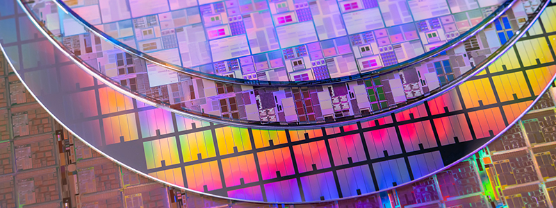
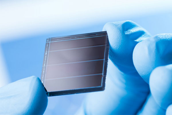
Semiconductor manufacturing requires extreme purity, as even ppt and ppq-level contaminants can impact performance. Traditional techniques struggle at the nanometer scale, but Agilent ICP-MS provides ultratrace elemental analysis with ppq sensitivity to ensure contamination control from raw materials to final product. Optimized for the semiconductor industry, it offers exceptional detection limits, interference removal, and seamless automation, making it a trusted choice for manufacturers globally.
Download this application compendium and get more than 20 methods to measure dissolved and particulate inorganic impurities in semiconductor manufacturing. The methods include instrument configuration and tuning parameters, sample and standard preparation details and representative results. The compendium is the ultimate guide to help you setup or refine your inorganic contamination testing program.
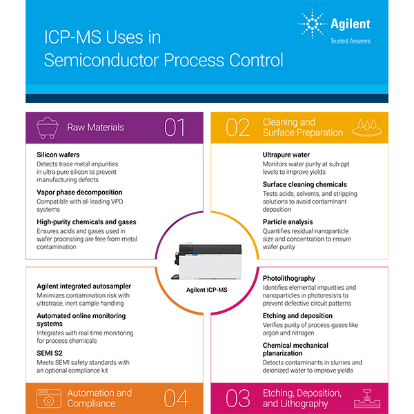
Our latest application notes offer valuable insights into ICP-MS analysis in semiconductor manufacturing, covering everything from silicon wafers to automation and compliance, helping you stay up-to-date with industry advancements.
The Agilent 8900
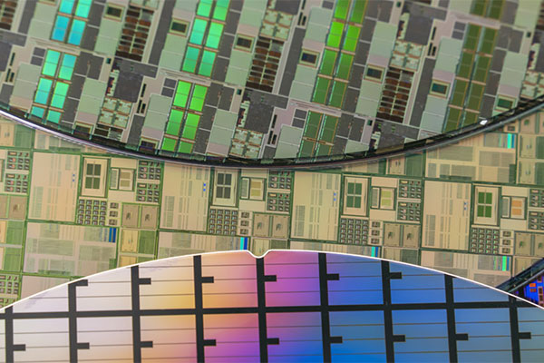
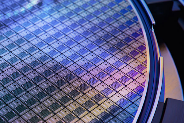
ICP-QQQ, integrated with IAS Expert PS vapor phase deposition (VPD), enables precise measurement of trace metals in both native and thermally oxidized SiO2 layers of silicon wafers, offering the sensitivity and reliability needed for continuous contamination control.
IAS Inc. has developed a new laser ablation (LA) ICP-MS technique using a femtosecond laser, Gas Exchange Device (GED), Metal Standard Aerosol Generation (MSAG_DS), and ICP-QQQ for direct analysis of whole wafers, overcoming challenges in conventional methods without requiring matrix-matched solid standards.
spICP-MS is a powerful tool for nanoparticle characterization, measuring particle number, concentration, size, and dissolved element concentration. In this study, SiO2 nanoparticles were analyzed in process chemicals using the 8900 ICP-QQQ in
spICP-MS mode.
Metal impurities in photoresist (PR) can impact semiconductor device performance. In this study, the 8900
ICP-MS/MS analyzed 20 trace elements in
IC-grade photoresist, achieving excellent precision and recovery for repeated measurements of a 0.1 ppb spike over an hour.
DE-004893
Please complete the form below to receive the latest resources in ICP-MS analysis in semiconductor manufacturing or to be contacted by an Agilent representative.